🔴 Website 👉 https://u-s-news.com/
Telegram 👉 https://t.me/usnewscom_channel
- SanDisk unveils High Bandwidth Flash (HBF), a NAND-based alternative to HBM
- HBF matches HBM bandwidth, offering 8–16x capacity at a lower cost
- SanDisk is planning to establish a technical advisory board of industry experts
It certainly seems as if splitting from Western Digital has lit a fire under Sandisk. At its recent investors day, the flash memory specialist look the wraps off super large SSDs, with the promise of even larger ones to come, and unveiled a new, cheaper DRAM alternative called 3D Memory Matrix.
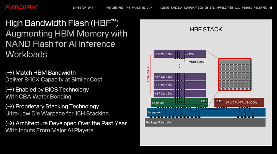
At the same event, Sandisk also unveiled its High Bandwidth Flash (HBF) concept which is taking aim at HBM by augmenting it with NAND flash to cater to AI inference workloads. Sandisk’s key objectives with HBF seems to be to match HBM bandwidth while providing 8–16 times the capacity at a similar cost.
According to a slide that Sandisk shared, HBF combines BiCS technology with CBA wafer bonding, allowing for efficient high-density stacking. The company has developed a proprietary stacking technology that reportedly delivers ultra-low die warpage, making it possible to achieve 16-die stacking without major structural issues.
Scaling up to 4TB
The architecture of HBF has been developed over the past year, with Sandisk incorporating input from “major AI players” (it doesn’t name names, sadly).
The diagram in the slide shows an HBF stack, which consists of multiple HBF core dies connected via TSV (Through-Silicon Via) and micro bumps, interfacing with a logic die and PHY, which then connects to a GPU, CPU, TPU, or SoC die. The entire stack sits on an interposer atop a package substrate, similar to the packaging design used in HBM.
HBF isn’t a straight drop-in replacement for HBM, but it does share the same electrical interface, so will only require minor protocol adjustments, according to Sandisk.
In another slide, a GPU with HBM providing 192GB of total memory, is compared with an alternative version combining HBF and HBM that increases the memory capacity to 3TB. A fully optimized setup with only HBF (which you can see at the top of the page) can scale up to an impressive 4TB.


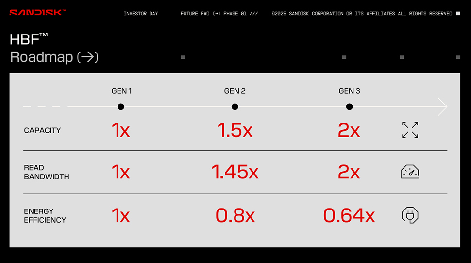
Sandisk’s HBF roadmap (below) shows how the company sees the technology advancing across multiple generations, focusing on capacity, read bandwidth, and energy efficiency. In the first generation, HBF establishes a baseline for these metrics. By the second generation, capacity is expected to increase by 1.5x, while read bandwidth sees a 1.45x improvement, and energy efficiency slightly decreases to 0.8x. By the third generation (there’s no indication of when Sandisk expects to arrive at this point), HBF is projected to double in capacity and read bandwidth compared to its initial version, with energy efficiency dropping further to 0.64x.
HBF is likely to receive some push back from rivals like Samsung and SK Hynix who are heavily invested in the $100 billion HBM market. Painfully aware of this, Sandisk is looking to establish an open standard ecosystem, and also a technical advisory board made up of industry experts and key partners.